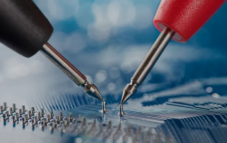
Why PCB Test Probes Matter in In-Circuit Test Setups
In-circuit test systems rely on mechanical contact to electrically verify each test point on a board. The effectiveness of the entire ICT fixture depends heavily on the performance of each board test probe installed inside it.
The Role of Probes in Test Accuracy
When a probe fails to maintain stable electrical contact, it can lead to intermittent readings, false failures, or undetected faults. In high-volume environments, inconsistent probe performance increases retesting cycles and affects overall throughput. Reliable PCB test probes help maintain stable electrical continuity, controlled compression force, and consistent readings across repeated test cycles.
For a deeper discussion on improving ICT measurement stability, you may refer to our article on board test probes and spring contact probes for test accuracy.
Board Test Probe vs Spring Contact Probes
A board test probe refers to the contact element that physically touches the PCB pad. Spring contact probes are designed with internal spring mechanisms to allow controlled compression. This compliance ensures consistent pressure even if board height varies slightly due to manufacturing tolerances.
In high-density ICT fixtures where hundreds or thousands of contact points are tested simultaneously, spring contact probes provide mechanical stability that rigid contacts cannot achieve.
Understanding Probe Stroke and Overtravel
Stroke is one of the most overlooked but critical specifications when selecting PCB test probes.
Working Stroke vs Total Travel
Working stroke refers to the compression range where the probe delivers stable spring force and optimal electrical contact. Total travel includes the maximum physical compression limit of the probe.
If a fixture design requires more compression than the working stroke allows, contact resistance may increase or the probe may bottom out prematurely.
Why Overtravel Matters
Overtravel provides the tolerance margin needed to accommodate minor PCB height variation or surface irregularities. Without sufficient overtravel allowance, PCB test probes may bottom out or fail to achieve proper compression, leading to unstable contact resistance.
Stroke specifications must therefore be aligned with overall fixture architecture. For additional insight into how probe compression interacts with fixture structure, you may refer to our discussion on in-circuit test fixtures for Keysight and Teradyne systems.
Spring Force and Contact Pressure
Spring force determines how firmly the probe presses against the PCB test pad.
Balancing Mechanical Stress and Electrical Stability
Low spring force reduces pad wear but may compromise contact reliability. Excessive force can damage delicate pads, especially in fine-pitch layouts.
Force selection should consider:
- Pad surface finish
- Pad size
- Expected compression cycles
- Board thickness variation
Selecting Spring Contact Probes for Fine-Pitch Boards
In compact PCB designs commonly seen in IoT and telecom equipment, small pads require carefully calibrated spring force. Excessive force may cause indentation or plating damage, while insufficient force leads to unstable resistance measurements.
Probe Tip Geometry and Surface Compatibility
Tip geometry directly affects contact performance and durability.
Common Tip Styles
| Tip Type | Application Use Case | Key Advantage |
| Crown | General ICT | Stable contact across flat pads |
| Spear | Fine pitch pads | Precise penetration |
| Concave | Rounded solder pads | Centered seating |
| Serrated | Oxidised surfaces | Breaks through contamination |
Different surface finishes such as ENIG, HASL, or OSP respond differently to tip styles. Selecting appropriate geometry reduces pad wear and improves signal consistency.
Matching Tip Style to Production Conditions
For boards exposed to oxidation or extended storage, serrated or sharper tips may provide better penetration. For delicate finishes, smoother crown styles may preserve pad integrity.
High Current Probes in Power Applications
Not all PCB test probes are designed to carry higher currents. High current probes are engineered with larger contact areas and stronger internal structures to handle increased load without excessive heat generation.
When High Current Probes Are Required
Power electronics, automotive modules, and battery-related PCBs often require testing under higher current loads. Using standard probes in these environments can lead to:
- Thermal buildup
- Increased resistance drift
- Reduced probe lifespan
Thermal Considerations
Higher current generates more heat. Properly rated high current probes minimize voltage drop and maintain electrical stability across repeated cycles.
Contact Resistance and Cycle Life
Two specifications that engineering teams should always verify are contact resistance and mechanical cycle life.
Contact resistance influences measurement precision. Stable low resistance values help ensure consistent readings.
Cycle life indicates how many compression cycles a probe can withstand before performance degrades. In high-volume production, probes may cycle thousands of times per day. Selecting probes with appropriate durability ratings prevents frequent replacements.
Common Procurement Mistakes
Even experienced procurement teams sometimes overlook technical compatibility.
Selecting on Cost Alone
Lower-cost probes may initially reduce procurement budgets but often result in shorter operational life and higher replacement frequency.
Ignoring Specification Alignment
Stroke, spring force, current rating, and tip style must align with fixture design. Mismatched specifications compromise reliability.
Overlooking Lead Time
Electronics manufacturing schedules in Singapore are tightly managed. Ensuring consistent supply availability is part of long-term fixture planning.
PCB Test Probes in Singapore’s Manufacturing Landscape
Singapore’s electronics sector demands precision, repeatability, and high production standards. Understanding probe specifications helps engineering and procurement teams make informed decisions.
As a Singapore-headquartered engineering company, Petracarbon supplies semiconductor probing components used in in-circuit test applications. We focus on reliable sourcing of PCB test probes, spring contact probes, interface probes, and high current probes for manufacturers requiring consistent quality components.
Final Considerations for Selecting PCB Test Probes
Selecting the right PCB Test Probes requires careful evaluation of stroke, spring force, tip geometry, current rating, and cycle durability. Each parameter influences the reliability of in-circuit test results and overall production efficiency.
By understanding these technical considerations before procurement, engineering and sourcing teams can build more stable fixtures and reduce unnecessary retesting cycles. Petracarbon supports manufacturers by supplying precision probe components suited for modern ICT environments, helping ensure reliable sourcing for long-term production needs. For sourcing enquiries or specification discussions, you may reach out via our Contact page.